Efficient Power Conversion at Solaires
How we hit 35% efficiency
Solaires Team | Victoria, B.C | April 30th, 2024
If you spend enough time looking at solar power, you will often find references to something called “power conversion efficiency”, shortened to PCE, which refers to the amount of power a solar cell can harness compared to the total amount of power they receive from light. Solar manufacturers highlight their PCE in their materials, and researchers consistently hype record PCEs for whatever set of conditions they are studying. Generally, these records boast PCEs between 20 and 30 %. You then may ask, just how efficient can solar cells get?
As we’ve discussed before, photovoltaic cells work by absorbing photons of light, which creates an electron/hole pair. The electron/hole pairs migrate to opposite ends of the cell, and out to a load which uses that charge to either power a device, or charge a battery. In that previous article, we discussed how the energy of photons that a semiconductor - the heart of photovoltaics - can absorb is dictated by its “bandgap”.
In sunlight, a single junction solar cell, which is to say a solar cell with only one photon absorbing material, is maximally efficient with bandgaps between 1.1 and 1.4 electron volts (eV). With eV, the higher the number, the higher energy the photon. So a 1.4 eV photon is in the infrared range, while a 2.4 eV photon would be in the green range of the light spectrum.
If you recall that a semiconductor can absorb light that is of its bandgap or higher energy, you may wonder why the ideal bandgap for photovoltaics would not be smaller than 1.1 eV. The fact is that below-bandgap photons are only one source of potential solar energy losses. With semiconductors with small bandgaps, electron/hole pairs are more likely to recombine and waste energy, which causes up to 20 % energy loss in an efficient solar cell. More importantly are losses due to vibrational relaxation. Generally, semiconductors do not provide more energy per photon than their bandgap. As a simplification, when high-energy photons create an electron/hole pair, the excited electrons will relax “vibrationally” until they reach the bandgap energy level. The interplay between a semiconductor’s bandgap, energy losses due to relaxation, below-bandgap photons, recombination, and the remaining power that can be used is described in the radiative efficiency limit diagram below.

Schematic diagram of the radiative efficiency limit. The black band represents percent usable electrical power (y-axis) for an outdoor solar cell for a specific bandgap (x-axis). Green band represents the losses due to thermal relaxation of photons (lost to heat). Pink band represents percent of sunlight that is too low energy to be absorbed by the solar cell. Blue band represents miscellaneous other losses, including recombination and energy losses during the transfer of charge from the solar cell to electrical contacts.
Attribution: Sbyrnes321, CC0, via Wikimedia Commons
From that figure, we can see that a single junction cell has a maximum efficiency of ~ 33.7 % in sunlight, but at Solaires, we are proud to promote that our single junction PVModules have reached 35 % efficiency! How are we reaching this limit? PVModules are specially designed not to absorb the sunlight, but to absorb indoor light; specifically, the visible spectrum that makes up the vast majority of indoor light. Sunlight contains a very broad spectrum of light wavelengths; from IR through UV. Engineers of artificial lights have no reason to include non-visible lights in their bulb emissions. Just look at the next figure to see how different the light spectrum for sunlight and many forms of artificial light are!
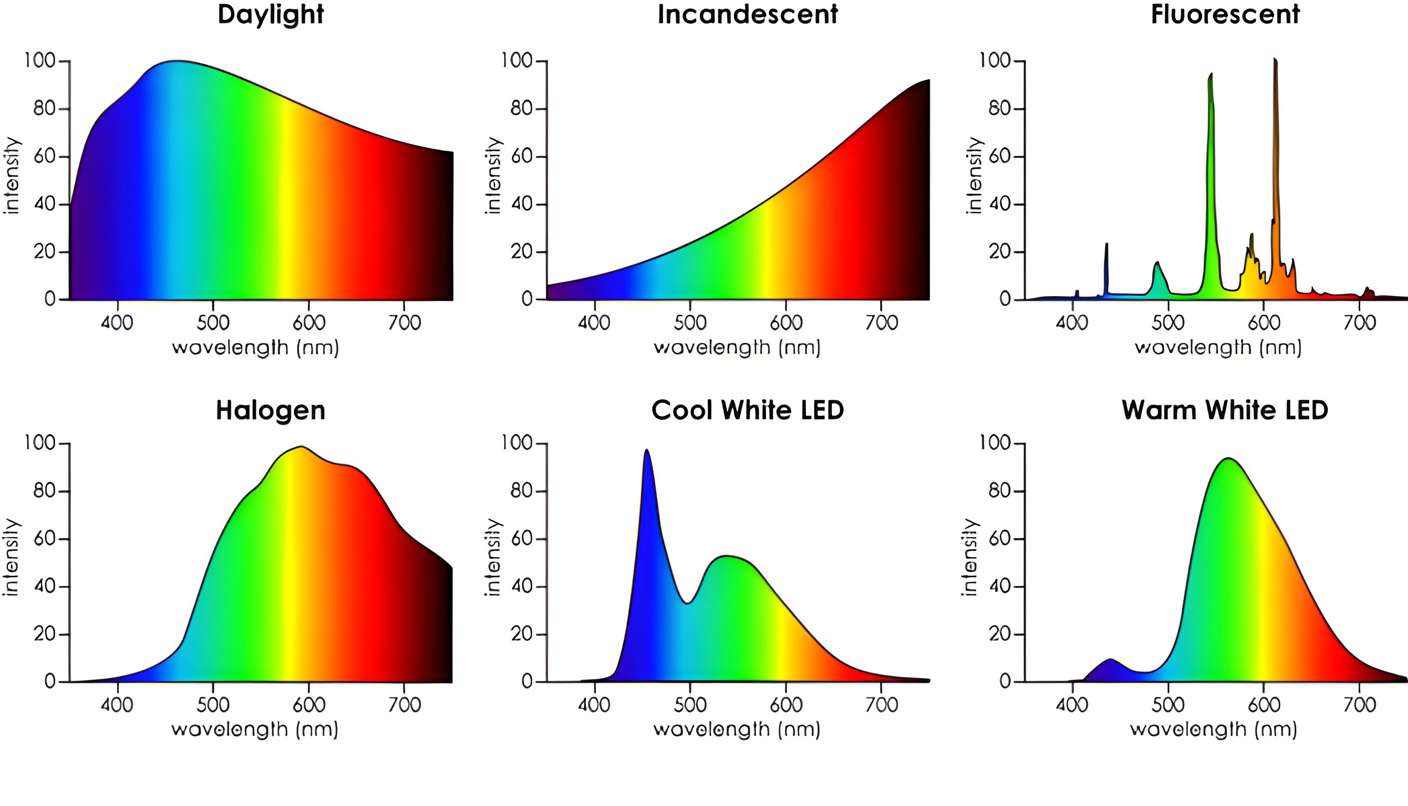
Schematic diagram of the relative intensities of visible light from different common sources. Attribution: Ondřej Růžička, https://www.lightingschool.eu/portfolio/understanding-the-light/
Remember that the optimal bandgap for outdoor PV is 1.4, well within the IR range of the light spectrum. This is because the long tail of sunlight where emissions lie deep into the IR spectrum and having a visible light bandgap would simply waste all of that IR light. With indoor light; however, very few IR photons are produced (with the exception of the now-rare incandescent lights), so we can use a higher energy bandgap semiconductor. At higher energy bandgaps, both recombination and relaxation losses are reduced, further improving theoretical efficiencies.
Adapting to the needs of the application is one of the core promises of perovskite technologies like our Solar Ink and our PVModules . Unlike metalloids like silicon, perovskites are a crystal class of chemicals which are very effective at absorbing light. While the bandgap of silicon can be tuned a few eV based on clever materials physics, we can greatly tune the bandgap of perovskite crystals by changing its chemical composition. For comparison, silicon PVs typically have bandgaps between 1.0 and 1.5 eV; all within the IR range. Meanwhile, perovskites can range all the way from 1.2 eV (IR) to 2.6 eV (blue), something that Solaires has eagerly exploited!
In the figure below, we compare the efficiency limits of indoor and outdoor PV cells. As you can see, indoor lights have a very high potential efficiency. In fact, our PVModules have been specifically designed to harness that high efficiency limit, exceeding 35 % now, and are soon to exceed 40 %!
Just because PVModules are designed to maximally absorb indoor light, that doesn’t mean they don’t work in sunlight. On sunny days, the amount of sunlight that reaches the earth’s surface is much, much more than even the brightest office buildings that we work in. Ambient daylight provides anywhere from 10 to 150 times as much light as you are likely illuminated indoors, so even though the indoor line of PVModules is less efficient in daylight, it still produces more power outside. In other words, devices tuned for indoors can work outdoors, but devices tuned for outdoors cannot be used indoors.
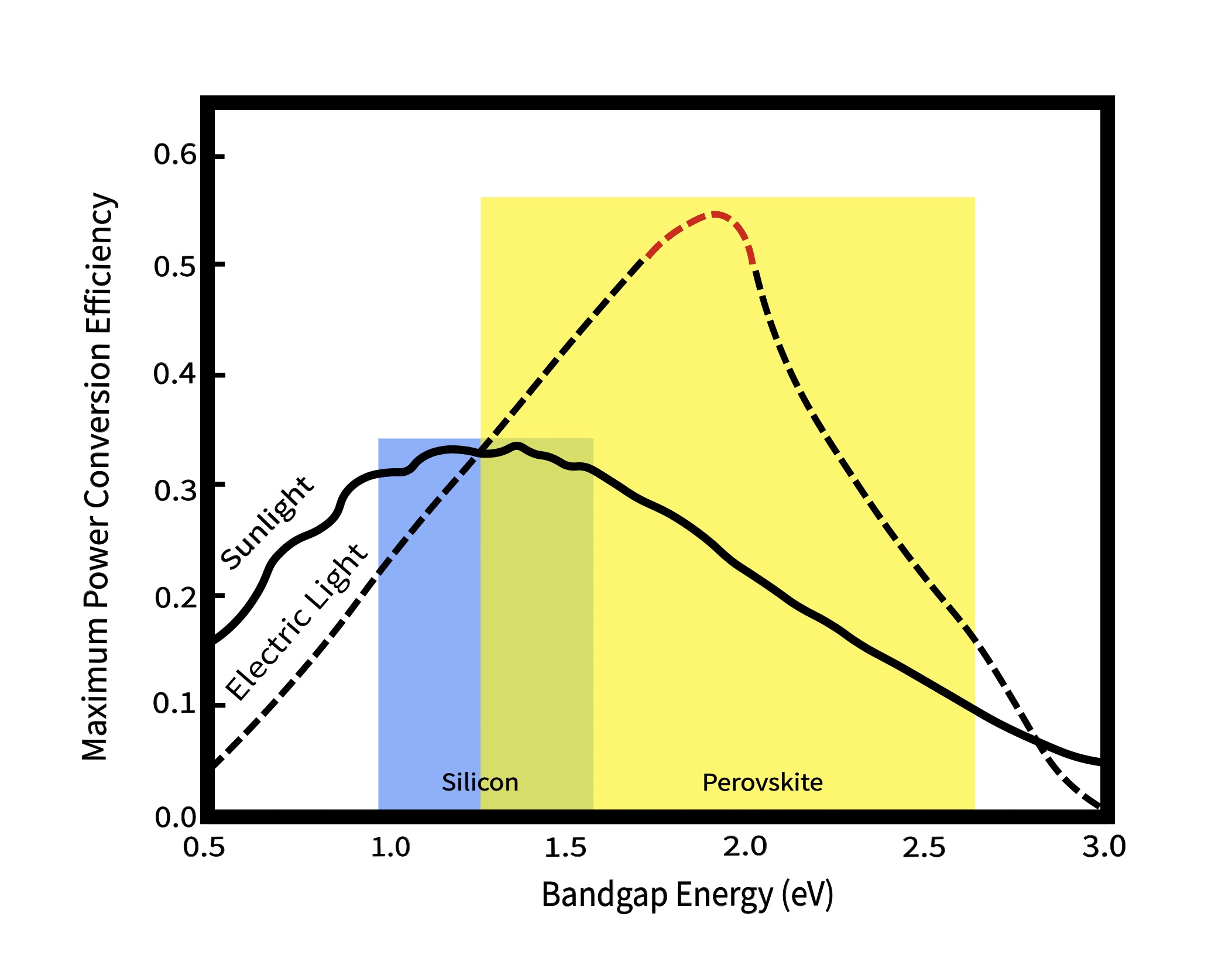
Schematic diagram showing the radiative efficiency limits for sunlight (solid line) and artificial light (dashed line). The range of possible eVs for silicon devices is shaded in blue. The range of eVs for perovskite devices is shaded in yellow. The eV range for PVModules is shown by a red box. Attribution: Solaires Enterprises Inc.
By tuning our PVModules towards indoor lights, we can power a wide range of IoT and consumer electronics. These include wireless keyboards, smart door locks, environmental sensors, and so much more! At Solaires we are excited to work with electronics manufacturers all around the world to power their devices with our PVModules. If you are a consumer of the latest and greatest technologies, keep your eyes on us for upcoming announcements about the devices where you can buy our products and participate in the perovskite revolution. If you are an electronics manufacturer, please contact us so we can discuss how we can work together to make the future of electronics greener and cleaner!