History of Solar Innovation: From Thin Films to Perovskite
From early innovations to cutting-edge perovskite
Solaires Team | Victoria, B.C | May 30th, 2025
At Solaires, we’re not just part of the photovoltaic revolution—we’re leading it. Our breakthrough perovskite technology marks the culmination of nearly two centuries of scientific discovery, unlocking new levels of efficiency, flexibility, and accessibility that silicon, the market leader, simply can’t match. It’s a transformation that redefines what photovoltaic energy can be: lightweight, adaptable, and built for the future. But to understand how we arrived at this moment, we have to start at the beginning. Where did the perovskite technology that powers Solaires’ industry-leading products come from? Going even further, how did we learn that when you shine light on some substances, they can generate electricity?
While the modern impression of solar panels comes from rigid silicon wafers, the photovoltaic effect (the generation of electrical current after light exposure) was first described in 1839 as a liquid. A 19-year-old Edmond Becquerel (father of Henri, a co-discoverer of radioactivity), discovered the photovoltaic effect in electrodes dissolved in silver solutions, in experiments driven by exciting advances in photography.
Little progress would be made for decades until the 1870s, experiments with bars of selenium began to demonstrate the photovoltaic effect in solids for the first time. Charles Fritt’s selenium solar cell in 1883 was the first solar cell in history, though it was only able to convert ~ 1 % of incoming sunlight to electricity. What followed were decades of excitement and false starts, as patents and proclamations were filed by inventors and con men alike. Mostly were based on selenium. None were commercially relevant.
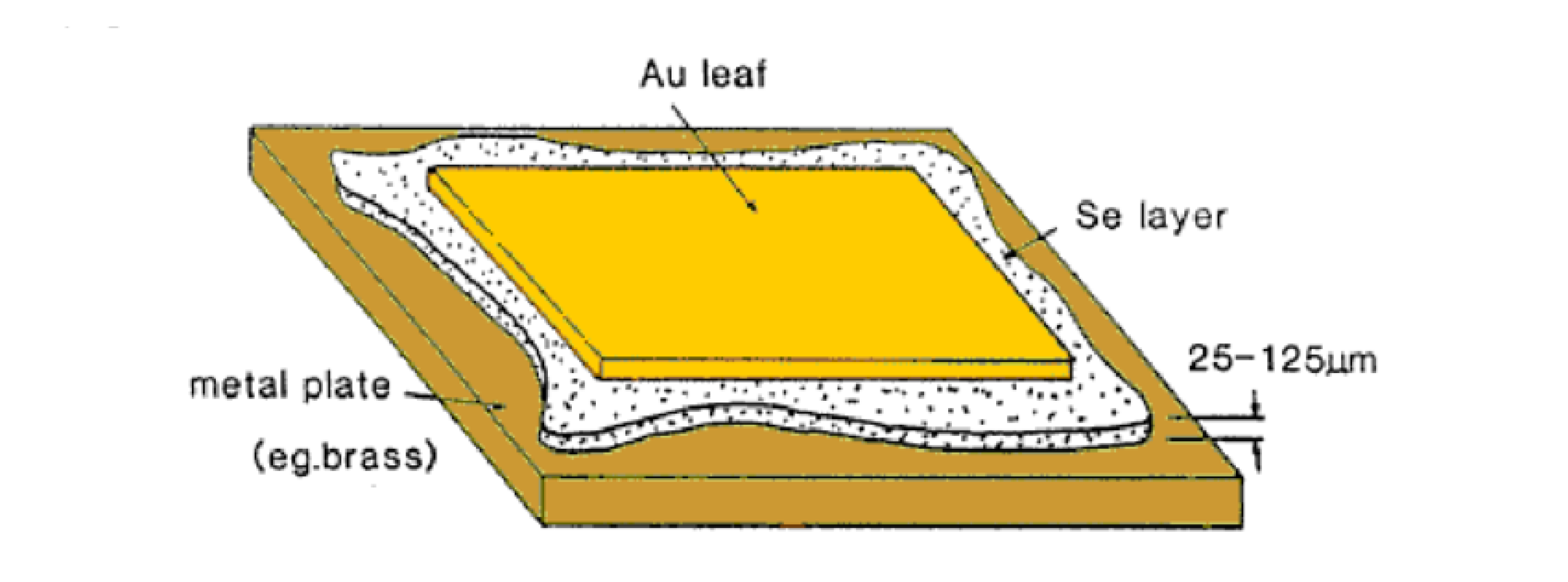
Schematic diagram of Charles Fritts’s first photovoltaic cell. A thin gold (Au) leaf is laid atop a layer of selenium (Se), which in turn is deposited on a metal substrate such as brass. The selenium layer, typically 25–125 µm thick, acts as the light-absorbing semiconductor. This metal–semiconductor–metal structure was the first practical demonstration of the photovoltaic effect in a solid-state device, developed in 1883. Fritts’s cell achieved an efficiency of about 1%, initiating the era of photovoltaic research.
Attribution: K.H. Böer, CC BY-SA 3.0, via Wikimedia Commons
Meanwhile, the theoretical understanding of photovoltaic technology was expanded, as the burgeoning solar field was intrinsically linked to the new field of quantum physics. Simultaneously, materials scientists developed new methods to produce robust semiconductors with never-before-seen purities. Most critical for the solar industry, Jan Czochralski’s method for producing single crystals of semiconductors was developed in 1915 and is still used today for producing extremely high-performance silicon ingots.
These worlds finally collided at Bell Labs in the 1940s and 50s, where solar cells evolved from selenium and germanium-based curiosities into the silicon-based marvels that electrify communities and power satellites. By the 1950s, silicon-based solar cells reached power efficiencies of up to 9 % and were showcased on Vanguard I, the USA’s second satellite and oldest human-made object still in orbit today. By the 1970s, silicon solar cells were an entrenched technology in spacecraft, where renewable power requirements trumped cost considerations. It took until the late 1970s for prices to drop below 75$ USD per watt and efficiencies exceeded 15 %, at which point commercial silicon panels were possible. From there, the story of silicon solar panels is that of increased production, decreasing prices, and technological innovation that has dropped the cost of solar cells to ~ 0.25$ USD per watt and efficiencies approaching 27 %. But just as wafer-based silicon solar cells began their commercial ascent, the second generation of solar technologies was being developed; the first thin-films.
Thin-film solar cells were developed on the promise that they could be flexible, require less material, be printed on a low-cost production line, and be extremely lightweight. The first generation of thin-film solar was developed in the early 1970s, with gallium arsenide (GaAs), copper indium gallium diselenide (CIGS), cadmium telluride (CdTe), and a thin-film version of silicon called amorphous silicon (a-Si) due to its non-crystalline structure. Development of these materials started in earnest in the 1970s, and by the 1990s, GaAs solar cells passed silicon as the best performing solar cells in the world, but they were then, and are now, hampered by extremely high production costs and prices due to the difficulty in manufacturing and raw material costs. Today, while GaAs can be found in commercial products, they mostly found their niche in space travel, where, just like silicon in the 1960s, performance (and weight!) takes precedence. Throughout the 1990s and 2000s, CIGS and CdTe technologies matured enough to produce solar modules with 15 - 20 % efficiencies and all of the benefits of lightweight solar cells. Unfortunately for these technologies, an investment boom in the 2000s coincided with the explosive growth of Asian silicon industries that pushed silicon solar panels from ~ 7$ USD per watt to less than 1$ USD by 2013. Few thin-film companies were able to compete with these low costs, and by 2021, less than 5 % of the global PV market comes from second-generation solar technologies; though the USA does still have a notable (~ 30%) CdTe market share. The problem with the second generation of solar was the inability to produce solar cells as effective or as cheap as silicon. GaAs, CdTe, and CIGS costs are inflated by expensive production techniques and tight supply chains. For example, nearly half of the world’s tellurium is already used in solar cells, despite its low market cap. While GaAs produces extremely high-efficiency (and high-quality) solar cells at a high cost, CdTe and CIGS devices are far less efficient than silicon.
The third generation of solar cells aims to marry the high performance of silicon solar cells with the thin-film applications of the second generation; with the most notable coming from dye-sensitised solar cells (DSSCs), organic photovoltaics (OPVs), and perovskites (PSCs). The theoretical basis of DSSCs goes back to photographic research in the 1880s, and DSSC-related work continued throughout the early to mid-20th century. Modern DSSCs were developed in the late 1980s and early 1990s by Michael Grätzel and Brian O’Regan at UC Berkeley and EPFL in Switzerland. DSSCs work by doping the surface of a highly conductive, low-cost semiconductor (usually titanium dioxide) with a photoactive dye that “injects” photo-excited electrons into the semiconductor to generate an electric charge. The electrons are recovered from a redox shuttle, typically a liquid iodine buffer. The whole process was not dissimilar from how photosynthesis works in plants. Alongside DSSCs, several other thin film solar cells have been developed since the early 2000s, often alongside advancements in screen displays made of similar materials, like organic photovoltaics and quantum dot solar cells (QDSCs), or the CIGS-like films, including copper zinc tin sulfide solar cells (CZTSSCs).
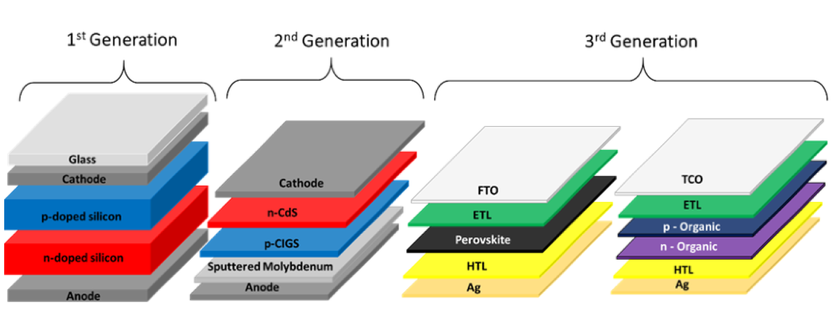
The 1st Generation uses thick silicon layers, the 2nd Generation uses thin films like CIGS, and the 3rd Generation includes newer materials like perovskites and organics. Each generation aims to reduce costs and improve efficiency.
Attribution: Umar, A. & Alothman, Z.A. (2024), CC BY 4.0, via ResearchGate.
Within a decade of their discovery, EPFL scientists had produced ~ 10 % efficient DSSCs, but two decades later, DSSCs were limited to efficiencies < 12 %. In order to both reduce costs and explore performance gains, a broad panel of artificial dyes were used to absorb light, replacing traditional ruthenium-based dyes. In 2009, Tsutomu Miyasaka’s group incorporated perovskite dyes into a DSSC structure and showed low, but promising quality. After exploring the possibilities of perovskite-based DSSCs, Miyasaka’s group worked with Michael Snaith’s research team at the University of Oxford and showed that perovskite solar cells without TiO2 (a core component of DSSCs) exceeded the performance of solar cells with perovskite as a DSSC dye on TiO2. Their development kicked off the field of perovskite solar cells. Within a year, perovskite solar cells were beating the performance of DSSCs, OPVs, and a-Si. By 2018, improvements in perovskite printing methodology and materials optimisation pushed power conversion efficiencies above 20 %, and higher at the time than the best CIGS, CdTe, and polycrystalline silicon modules. And now, in 2025, the best perovskite solar cells have efficiencies of > 26 %; only a couple of percentage points shy of the best single junction (i.e. only one film absorbing light) modules (GaAs and monocrystalline silicon), despite the > 40 year head start those two technologies have on perovskites.
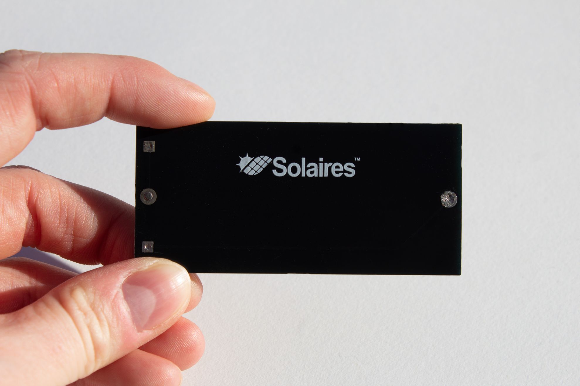
This PVModule uses next-generation materials to convert sunlight into electricity, aiming for lightweight, flexible, and efficient energy solutions.
Attribution: Solaires Enterprises Inc.
Today, the best DSSCs, OPVs, QDSCs, and CZTSSCs have peak power conversion efficiencies between ~ 15 % and 19 %, far below silicon and perovskite, and below even CdTe and CIGS. Furthermore, they lack the long-term stability that utility markets demand. What these technologies generally benefit from is the diversity of materials that can make up their architecture, allowing manufacturers to tune the optimal light absorption wavelength, just like we do at Solaires. This tunability has pushed commercial development towards the indoor applications, as DSSCs, OPVs, and perovskites are some of the most advanced artificial light absorbers in the world. Despite ongoing challenges in maintaining long-term stability of these emerging technologies, their integrated devices (IoT sensors and consumer electronics) are not required to be in use for 25 years, as utility scale solar solutions demand.
For all the advancements that perovskites have made in the last 15 years, challenges remain on the road to commercial adoption. The two largest are long-term stability in harsh outdoor conditions and scaled production to reach the mass market. As such, the indoor and consumer electronics markets are a critical springboard to provide experience and consumer trust in perovskites, while we prove that we can scale up, improve performance, and reduce costs.